Table of Contents
The DL0102GXN (“GXN”) can be configured for external HIVDC (Tx/pulse voltage) control. Here are the operating methods and parameters.
Overview
The DL0102GXN (“GXN”), and all the (H)DL devices for that matter, can be modified for R&D purposes with a set of IC pin sockets to allow quick swapping of the high-voltage (HIVDC) module for different devices within a series. The output (HIVDC/Tx) voltage for a given control voltage depends on the module.
The GXN has the option to use a pin on the board to externally and manually set the control voltage for R&D purposes.
Use a stable, regulated, bench supply to generate the control voltage. Ideally digital control will probably yield the most repeatable control voltage. Current is typically < 50 mA.
Connections & Equipment
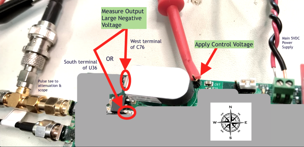
The ground for the bench supply for the control voltage should be tied to the input main GXN power supply (5VDC / USB).
The bench supply output positive voltage should be connected to the JP3 single-pin header near the HIVDC supply module.
Use a DMM capable of measuring up to about -500VDC or more (most do) with some good amount of reliability, and double-check your range setting before operating the GXN with external control voltage.
When probing the board for HIVDC, use very fine tipped probes.
Bounding Parameters for the Operating Envelope
For a GXN modified for larger Tx voltages, the output voltage should generally not be set to greater than (more negative than) -400VDC, and probably lower for some situations where XD terminations and cable-XD interactions might send a larger voltage to the crystal (risking crystal damage) or the “ring-back” reflection and inductance might create a total peak-to-peak voltage larger than 800V (ideally less). In some very carefully planned cases, you could probably use near -500VDC. Greater R&D voltages will require some updates or revisions to the board.
In bench testing here, these control voltages (maximum values) were used for controlling a -500V module:
| Bench Supply (VDC) | HIVDC Output (VDC) | Condition |
| 3.7 | -221 | Simulate “stock” conditions |
| 4.7 | -285 | [Conditional Maximum] Termination conditions (no-L) where the XD crystal may see voltages greater (more negative) than the Tx voltage itself (see details in presentation elsewhere) |
| 6.1 | -382 | [Conditional Maximum] Termination conditions (L) where the peak-to-peak voltages at the board connector far exceed the negative Tx voltage itself |
Photo and Diagram
